Circuit boards, the nerve centers of the electronic world, are intricate mosaics of technology that power everything from the simplest gadgets to the most complex computing systems. Understanding the anatomy of these essential components offers insight into how electronic devices function and communicate. This article explores the foundational elements of circuit boards, from the chips that process information to the circuits that connect everything together, shedding light on the inner workings of modern electronics.
Contents
- The Backbone of Electronics: Printed Circuit Boards (PCBs)
- Conductive Pathways: The Circuits That Connect
- Components: The Building Blocks of Functionality
- Soldering: The Art of Making Connections
- Multilayer PCBs: Complexity and Integration
- Surface Mount Technology (SMT) and Through-Hole Technology
- The Role of Vias in Multilayer Connectivity
- Testing and Troubleshooting: Ensuring Reliability
- The Future of PCB Design: Innovation and Integration
- Conclusion
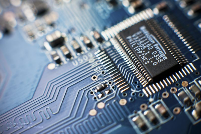
The Backbone of Electronics: Printed Circuit Boards (PCBs)
How do circuit boards work? At the heart of every electronic device lies a Printed Circuit Board (PCB). This base layer acts as the physical platform for mounting and connecting various electronic components. Made from non-conductive materials like fiberglass or composite epoxy, PCBs support conductive pathways, pads, and other features etched from copper sheets, facilitating electrical connectivity throughout the device.
Conductive Pathways: The Circuits That Connect
The conductive pathways, or traces, are thin lines of copper or another conductive material etched onto the PCB’s surface. These traces form the circuit, creating a roadmap for electricity to flow between components. The complexity and layout of these pathways determine the functionality and performance of the electronic device, making precision in design and manufacturing critical.
Components: The Building Blocks of Functionality
A variety of electronic components are mounted on PCBs, each serving specific functions within the circuit. These include:
- Resistors: Manage the flow of current, ensuring components receive the appropriate power level.
- Capacitors: Store and release electricity, helping to stabilize power supply and filter noise.
- Inductors: Store energy in a magnetic field, used in filtering and energy storage.
- Transistors and Integrated Circuits (ICs): Act as switches or amplifiers for electrical signals, with ICs combining multiple transistors and other components into a single package for complex processing tasks.
- Diodes: Allow current to flow in one direction, protecting the circuit from reverse currents.
The arrangement and interaction of these components define the circuit’s capabilities, from simple light switches to sophisticated computers.
Soldering: The Art of Making Connections
Soldering is the process of permanently attaching components to the PCB. By melting solder (a metal alloy with a low melting point) around the connection points, components are securely and electrically connected to the board. This technique requires precision to ensure reliable connections without damaging components or creating short circuits.
Multilayer PCBs: Complexity and Integration
As electronic devices have become more complex, so too have the PCBs that drive them. Multilayer PCBs consist of several layers of substrate, each with its conductive pathways, separated by insulating materials and pressed together. This design allows for more circuits to be packed into a compact space, supporting advanced functionalities in modern electronics.
Surface Mount Technology (SMT) and Through-Hole Technology
Two primary methods are used to attach components to PCBs: Surface Mount Technology (SMT) and Through-Hole Technology. SMT components are placed directly onto the surface of the PCB and soldered to pads, allowing for smaller components and denser circuit layouts. Through-hole components, on the other hand, are inserted into drilled holes on the PCB and soldered to pads on the opposite side, providing stronger physical connections suitable for larger components or those subjected to mechanical stress.
The Role of Vias in Multilayer Connectivity
Vias are small holes in the PCB filled or plated with conductive material, allowing electrical connections between different layers of a multilayer PCB. These essential features enable the complex routing required in densely packed circuits, facilitating communication and power distribution throughout the device.
Testing and Troubleshooting: Ensuring Reliability
Once assembled, PCBs undergo rigorous testing to ensure they function as intended. This process involves checking for shorts, open circuits, and proper functionality of components. Troubleshooting faulty PCBs requires a systematic approach, often starting with visual inspections and followed by more in-depth electrical testing to pinpoint the issue.
The Future of PCB Design: Innovation and Integration
The future of PCB design holds exciting prospects, with ongoing advancements in materials science, manufacturing techniques, and component technology. Innovations such as flexible PCBs, which can bend and flex, open new possibilities for wearable technology and devices with unconventional shapes. Similarly, the development of more efficient and smaller components continues to push the boundaries of what’s possible, enabling the creation of even more powerful and compact electronic devices.
Conclusion
The anatomy of circuit boards reveals a complex and fascinating world of technology that underpins the functionality of modern electronic devices. From the conductive pathways that form the circuits to the components that execute tasks, each element of a PCB plays a crucial role in bringing electronic innovations to life. As technology continues to evolve, the science and art of PCB design and manufacturing will remain central to the development of new and improved electronic devices, powering the future of technology.